International. Sony announced the launch of two types of event-based stacked vision sensors. These sensors designed for industrial equipment are capable of detecting only subject changes and reach the industry's smallest pixel size*1 of 4.86 μm.
Event-based vision sensors asynchronously detect luminance changes for each pixel and emit only the modified data, combining it with information about pixel position (xy coordinates) and time, allowing high-speed, low-latency data output.
The two new sensors employ stacking technology that leverages Sony's patented Cu-Cu connection*2 to achieve the industry's smallest * 1 pixel pixel size of 4.86μm. In addition to operating with low power consumption and offering high-speed, low-latency, and high-resolution temporal data output, the new sensors also feature surprisingly high resolution for their small size. All these advantages combine to ensure the immediate detection of moving subjects in various environments and situations.
These two sensors were made possible by a collaboration between Sony and Prophesee, combining Sony's CMOS image sensor technology with Prophesee's event-based vision detection technology. This enables high-speed, high-precision data acquisition and contributes to improving the productivity of industrial equipment.
With the increasingly sophisticated and diversified needs of the industrial equipment business,
the use of sensors to extract the necessary information from the images captured by cameras continues to grow, which demands an increasingly efficient data acquisition.
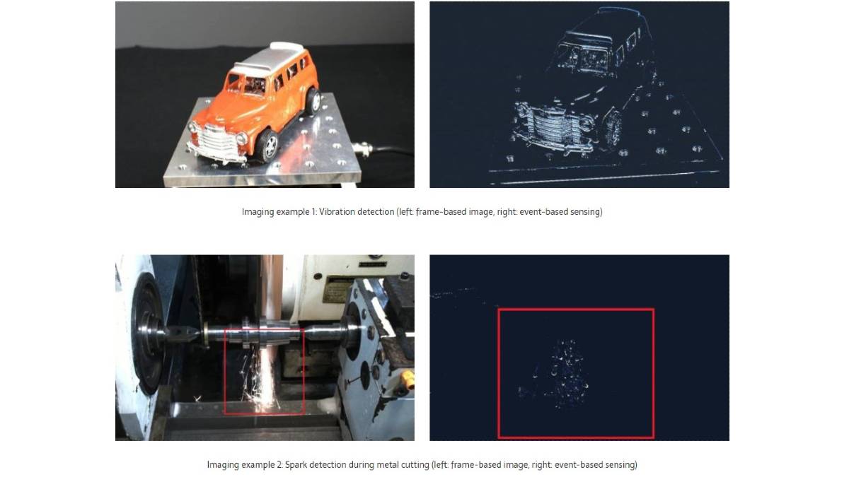
With the commonly used frame-based method, the entire image is output at certain intervals determined by the frame rate. However, Sony's new sensors use an event-based method that asynchronously detects pixel luminance changes and emits data with pixel position (xy coordinates) and time information.
They employ a proprietary stacked structure that leverages the Cu-Cu connection to achieve conduction between the pixel chip and the logic chip, which is equipped with a signal processing circuit to detect luminance changes, for each pixel. This design makes it possible for only pixels that have detected a change in the object's luminance to generate data, allowing the sensor to immediately detect luminance changes with high speed, low latency, and high temporal resolution while operating with low power consumption. Meanwhile, the design boasts the industry's smallest 1-pixel size* of 4.86μm, making it a very compact, high-resolution sensor.
These products can detect slight changes in vibration, detecting anomalies for use in predictive equipment maintenance. They also detect changes in sparks produced during welding and metal cutting, information that can be used to notify workers of the optimal time to change tools, among other possibilities. They can also help improve production in a variety of applications where frame-based image sensors struggle, as well as support work processes that rely on human experience.
* 1: between event-based stacked vision sensors. According to Sony's research (as of the announcement of September 9, 2021).
* 2: Technology that provides electrical continuity through Cu (copper) pads connected by stacking the pixel section (top chip) and logic circuits (bottom chip). Compared to wiring through silicon through (TSV), where connection is achieved by electrodes intruding around the circumference of the pixel area, this method brings more freedom in design, improves productivity, allows for a more compact size, and increases performance.
Source: Sony.