
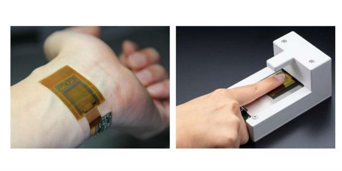
 International. The School of Engineering of the University of Tokyo and the company Japan Display have developed a thin image sensor that allows high-speed reading and high-resolution imaging through R&D together with the Someya Group of the Department of Electrical and Electronic Engineering of that school entity.
An image sensor is a type of imaging device, a two-dimensional sensor that converts light signals into electrical signals.
The integration of low-temperature polysilicon thin-film transistors with high-mobility, high-sensitivity organic photodectors has made it possible to create a single sensor that measures not only the distribution of pulse waves, which requires high-speed reading, but also biometric information, such as fingerprints and veins, which require high-resolution images. At just 15 micrometers thick, the sensor is lightweight and flexible.
As for biometric authentication, the sensor is expected to be applied to high-security authentication systems to avoid imitations and impersonations when obtaining biometric information (fingerprints and veins) and biometric signals (pulse waves).
The results of the research were published in the online version of the British scientific journal Nature Electronics on 20 January 2020. The research was supported by the JST-Mirai Program Small Start Type (ACCEL large-scale research) (JPMJMI17FI) of the Japan Science and Technology Agency (JST).
Source: Japan Display, Inc.


Leave your comment