
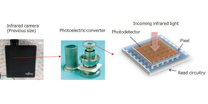
 International. A miniaturized photodetector for high-sensitivity infrared cameras was developed by Fujitsu Limited and Fujitsu Laboratories Ltd. In the future, this advanced sensor technology will allow infrared cameras to only be one-eighth the size of previous models, capable of taking detailed images even at night or at a distance.
There are considerable expectations surrounding the use of high-sensitivity infrared cameras in the navigation of ships under human observation. These cameras can take high-resolution images from a distance of up to six nautical miles (about 11 kilometers) during the day or night. However, the photodetectors in these cameras are still susceptible to thermal noise and, as the equipment required to cool them is quite large, it became necessary to find a way to reduce the cameras to a practical size. With the development of a semiconductor sensor structure that reduces the impact of thermal noise, Fujitsu Laboratories has made it possible to create hand-sized, high-sensitivity infrared cameras. In addition to this breakthrough, Fujitsu Limited has applied AI technology to process images taken with infrared cameras, and managed to automatically identify ships sailing up to six nautical miles away.
With high-sensitivity miniaturized infrared cameras installed around a ship's circumference, this enhanced technology will enable the identification of distant vessels without false positives.
Issues
When looking for cameras capable of taking highly detailed images, even at night or at a distance, attention has been focused on high-sensitivity infrared cameras, which are capable of capturing images at about twice the distance of normal infrared cameras. However, high-sensitivity infrared cameras absorb infrared light through photodetectors susceptible to thermal noise, so it is necessary to maintain an extremely low operating temperature of about 95 K (about -178 °C). The need for powerful cooling equipment for the photodetector has made the cameras relatively large, making them unsuitable for use in applications that require the installation of multiple cameras for full surround monitoring, even on board ships. Consequently, in order to improve the safety of navigation and control the surroundings of a moving ship without blind spots, it was shown that it was necessary to reduce the size of the cameras as a whole. For this reason, the increase in the operating temperature of the photodetectors and the reduction of the load of the refrigeration equipment represented a major problem.
About the newly developed technology
Fujitsu Laboratories has now developed a semiconductor structure that can raise the operating temperature of the photodetector without reducing its sensitivity compared to existing high-sensitivity infrared cameras.
The photodetectors of high-sensitivity infrared cameras directly convert the absorption of infrared light into electrical signals. During this conversion, thermal energy absorbs energy absorbed by infrared light and foreign electrons, generating unwanted electrical signals (thermal noise).
Thermal noise consists of two components: this includes noise that occurs around the edges of the sensor, specifically at the interface between the sensor and the protective layer covering its edges, and noise that occurs within the sensor itself. This newly developed technology reduces defects in the interface with the protective layer, which forms at low temperatures. Meanwhile, the electrical charge contained in the protective layer is controlled to prevent unwanted charging of the interface, which limits the thermal noise of the environment caused by defects and the concentration of the load.
In addition, Fujitsu Laboratories has reinforced the thermal noise resistance of the electron collection layer that connects to the absorption layer, which consists of alternating layers of semiconductor thin films of indium arsenide (InAs) and gallium antimony (GaSb). The region of the electrical junction (1) that is the source of thermal noise within this component has also shifted from the contact surface between the electron collection layer and the absorption layer to the reinforced electron collection layer, effectively reducing the volume of thermal noise within the sensor.
With these two technologies, Fujitsu was able to raise the practical operating temperature of the photodetector by more than 50°C over the previous technology, to 145K (about -128°C), making it possible to reduce the overall size of the camera, including the cooling component, to about one-eighth of its previous size.


Leave your comment